Metallic Coatings
Sputtered Molybdenum Films
The metal molybdenum is characterized by a high stability against thermal and mechanical stress and good chemical resistance. In addition, this metal has a very low specific resistivity. Due to the almost unique combination of these properties, molybdenum plays a special role among the sputtered metallic thin films. Therefore, these layers are used as sophisticated electrical contact material. Examples are printed circuit board tracks in microelectronics or back contacts for copper indium diselenide (CIS) solar cells, where molybdenum acts simultaneously as a diffusion barrier. Furthermore, molybdenum layers are also used successfully in multilayer systems for X-ray optics (mirrors) due to their low surface roughness.
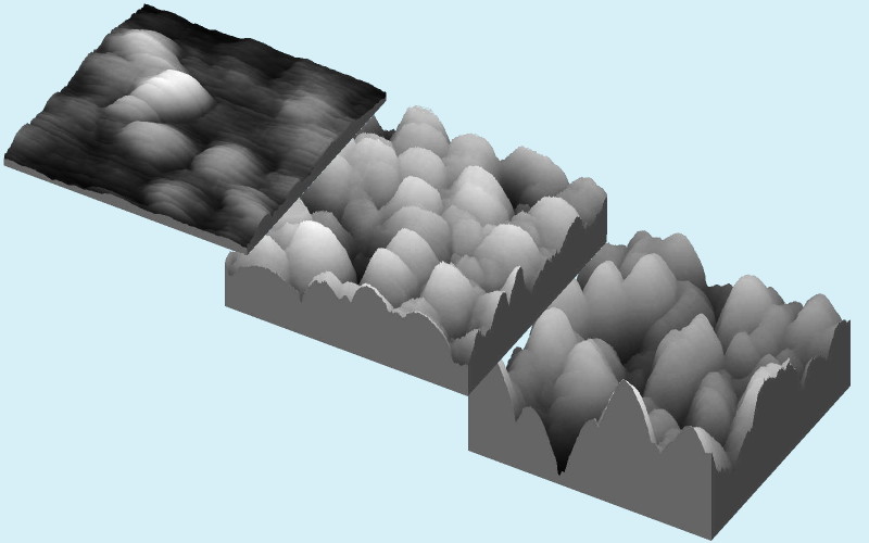
By properly selecting the coating temperature and optimizing the process parameters during sputtering (in particular, the thermalization of sputtered atoms and reflected argon atoms), thin layers with a density and resistivity close to bulk material values of 10,2 g/cm3 and 6 10-6 Ohm cm, respectively, are deposited. Under proper selection of sputtering parameters, these molybdenum layers show a very low surface roughness, which increases only slightly with film thickness (see below).
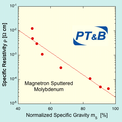
Left: The density of a sputtered molybdenum layer is influenced by the parameters of the sputtering process. The conductivity of these layers depends exponentially on their specific gravity (normalized to bulk material). Molybdenum layers with a density of 50% are highly porous (due to so-called nanovoids) and have a fractal dimension of 2.4.
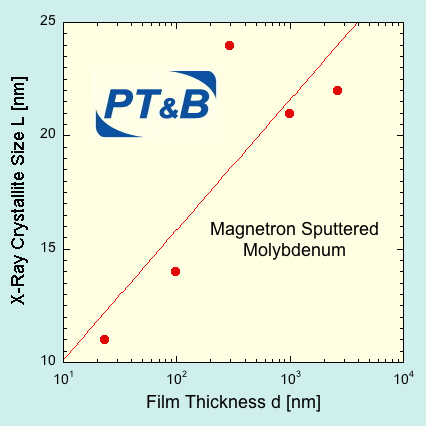
Right: The molybdenum in thin films consist of a fine crystalline material (“nanocrystallites“), the size of the crystallites increases approximately with the logarithm of the thickness of molybdenum.
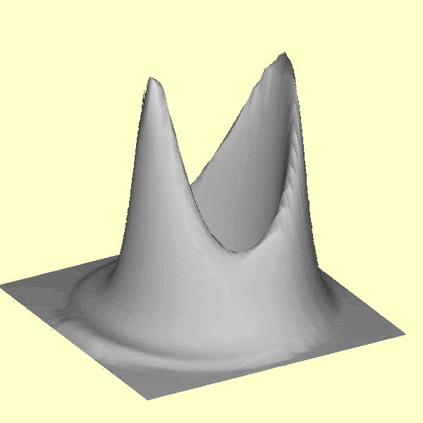
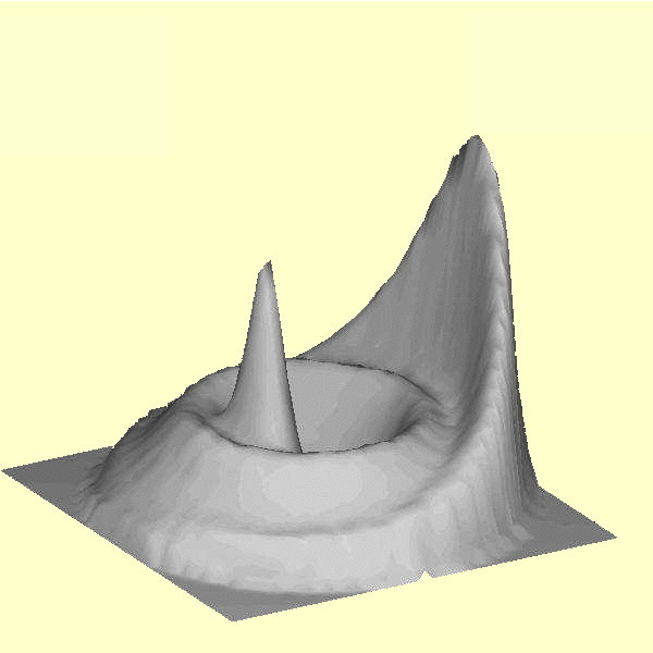
So-called pole-figures of x-ray wide-angle scattering (referred to as “omega-phi scans“) of the line corresponding to the (110) plane of the cubic body-centered molybdenum lattice. The layers deposited by means of magnetron sputtering usually show a fiber texture, which means that a particular axis of the crystallites is aligned parallel to the layer normal. Under bombardment of the growing film by argon and molybdenum atoms from preferred spatial directions, this fiber texture is disturbed (left). By further focusing of the impinging particles, an increasing orientation of the crystallites takes place also parallel to the layer plane and the texture becomes increasingly mosaic-like (right).
Publications on sputtered molybdenum films with PT&B SILCOR GmbH staff involved
- T. Drüsedau, F. Klabunde, M. Löhmann, and J. Bläsing: "A novel type of texture in molybdenum thin films", phys. stat. sol. (b) 196 (1996) K21-K23
- F. Klabunde, M. Löhmann, J. Bläsing, and T. Drüsedau: "The influence of argon pressure on the structure of sputtered molybdenum - from porous amorphous to a new type of highly textured films", J. Appl. Phys. 80 (1996) 6266-6273
- T. Drüsedau, F. Klabunde, P. Veit, and T. Hempel: "Investigations on microstructure, surface topography, and growth process of sputtered molybdenum showing texture turnover", phys. stat. sol. (a) 161 (1997) 167-184
- H.-M. Latuske and T. P. Drüsedau: "Electronic transport by ultrathin molybdenum layers buried in amorphous silicon", Phys. Rev. B 58 (1998) 10933-10941
- M. Löhmann, F. Klabunde, J. Bläsing, P. Veit and T. Drüsedau: “Structural investigations on ultrathin Mo-layers in a Si:H with emphasis on the island-continous layer transition”, Thin solid films 342 (1999) 127-135