Technologies
The Technology Sputter-Deposition
History of Sputtering
The effect of cathodic sputtering was first described in 1852 by the English physicist Grove. In the sixties of the last century very extensive basic physical investigations of this phenomenon were carried out. After several years, these resulted in an independent branch of thin film technology. Today the deposition of thin films by means of sputtering is a firm component of many production processes. Important operational areas of the sputtering technology are optics (e.g. architectural glass, reflectors, lenses), optoelectronics (solar cells, photodiodes, liquid crystal displays - LCD), electronics (e.g. microchips,), the memory technology (e.g. laser discs, magneto-optical media), the surface protection (tools, machine parts) or the barrier technology (diffusion barriers for example in flexible packing). The terms sputtering, sputtered films, sputter PVD or sputter coating are usual synonyms for this technology.
The physical mechanism of sputtering
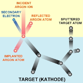
Left side illustration: The ions of the plasma (commonly of the noble gas argon) hit the negatively biased cathode (also referred to as target) with a high energy. There they collide first with an atom of the cathode material (primary collision). As is the case for the first break of a billiard game, the knocked atom transfers its momentum to the neighboring atoms of the cathode (secondary collisions). By the following further collisions, a so-called collision cascade develops. This leads under reversal of the original momentum direction to the emission of near surface atoms (sputter ejection). These sputtered atoms are the source of the film growing film. Two other effects influence the film growth. A part of the argon ions is reflected (dependent on the atomic mass of the target) in the form of atoms. During the transformation of the incident ions into atoms (recombination) secondary electrons are generated, which contribute to the preservation of the plasma.
The transport of sputtered atoms
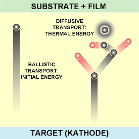
Right side illustration: The sputtered atoms possess a preferred direction perpendicularly to the target surface. They are of a high kinetic energy according to velocities between some km/s up to some 10 km/s. For the case of low pressures (or small distances between target and workpiece), the atoms reach the growing film without collisions with argon atoms of the sputtering atmosphere. They remain their initial high energy, what is referred to as “ballistic transport”. For high pressures (and large distances) the atoms suffer a multiplicity of collisions and are completely slowed down (“thermalized”). Their “memory” of the original flight direction is lost and they spread out evenly into all directions in space (diffusive transport). Therefore, the product of pressure and distance possesses a substantial influence on the characteristics of sputtered films.
Technical realization: Magnetrons
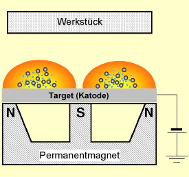
The use of sputtering for technical applications becomes only possible by means of sputter magnetrons (also referred to as magnetron source or briefly magnetron). In the simplest case of the planar circular magnetron, a central magnet is connected with a ring magnet by a yoke. The target has the shape of a circular disk. The magnetic field above the target develops in form of a half torus (similar a cut open donut). In this magnetic field the secondary electrons (blue) are caught generating ions (grey) and thus the plasma.

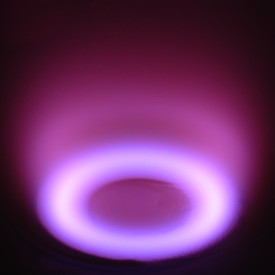
Due to the effect of the magnetron, the deposition rate increases (as a function of the target material) to values up to some 10 µm per hour. The pressure of the sputtering process can be lowered down to some hundredths of Pascal (Pa). As targets all elements and especially metals and semiconductors are suitable. It is also possible to use chemical compounds as oxides, nitrides or carbides for targets. By addition of gases as, e.g. Oxygen or Nitrogen to the sputtering atmosphere, these compounds can also deposited by means of elemental targets. The latter process is referred to as reactive sputtering.